While I am waiting for the
Eye's PCB
to arrive, I thought it best to start designing the head.
I want the head to be able to rotate continually in a direction, so I will be
adding a slip ring to the base of the neck to pass wires through from the main
body.
The slip ring enables the wire to be rotated without getting tangled up.
I want the head to nod as well as rotate, I will be using two small geared 6
volt motors.
To control these two motor I am using a cut down driver board I made for the
Arms.
As I am using DC motors I need to make some thing to give feedback as to the
position of the neck rotation and nod position.
To do this I am going to make similar sensors I used with the
Arms.
I will be using Magnets and the 3144 Hall Effect Sensors.
For the Neck Plate on which every thing rotates, I have placed Magnets all
around the edge.
I set the magnets in place with UV glue, this is a resin, so when it cured I
was able to sand it down to a smooth even surface the 3144 Hall Effect Sensor
could rest upon..
Next was the base of the head, I want the head to be able to look up and
down. This part also needs limit switches, so that the base of the head
does not hit the rotation platform.
The rotary platform also requires a sensor to detect when looking forward, so
that this position can be set.
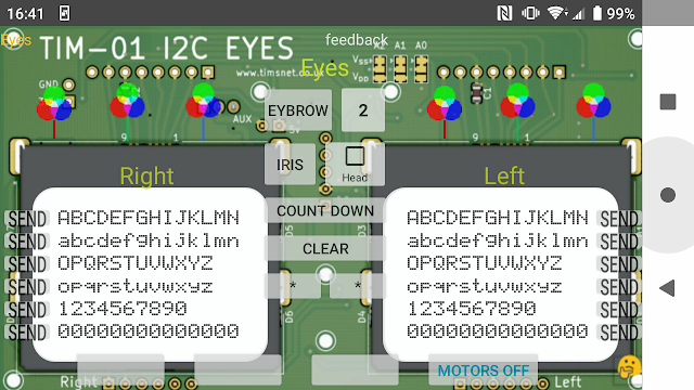
I have done a simple program to check some of its movements so far.
So far I have only done ASCII characters 32 to 127.
The 2x16 screen is the Chinese version, (Character Patterns - ROM
Code: A00) which has Chinese characters after ASCII number 61. There
are no characters between ASCII 127 and 60.
As for the Nokia Screens, I have only created ASCII characters 32 to
126 in the Arduino Library I made for the TIM-01 EYES.
There are two types, one comes attached to a breakout board and the LPH7366
that does not.
The LPH7366 has a zebra ribbon connection, it also has nine pins internally
connected to this ribbon.
I intend to use the LPH7366 version, they are cheaper (I don't think people
know how to connect them), also I want to make a board specially for this
project.
I am going to design a board that takes two of these screens and will control
them from an
PCF8574 I2C device, so that I can control it through my I2C bus on my robot.
PCF8574 Module
When I design the eyes I want to give them colour.
I have also written an Arduino library so others can use it once I have
finished it.
Got some WS2812B Addressable LEDs.
I found it cheaper to get them as a strip.
I cut two sections from the strip and stuck them on a new prototype support.
>
I wanted to control the WS2812B Addressable LEDs through the PCF8574 I2C
device also. But I was not able to do this. The signal to the WS2812B has
a pulse width of 400 nanoseconds.
That's 400 billionth of one second, the PCF8574 is not fast enough to do the
switching at this speed.
This is not really an issue, it just means there is one extra wire for the
WS2812B LEDs and if I add more WS2812B LEDs, I can just add them to this wire.
It's not what I wanted to do so I had another look on the web and found some
other Addressable LEDs. SK9822, these work similar to the Nokia Screens so I have ordered 10 of these.
These have clock and data wires (2 wire).
These are just what I wanted, because they have a clock wire, I am able to
control them with the PCF8574 module, I am able to use the same clock wire I
am using for the Nokia Screens, the data wire is a separate one.
(In hindsight I think I could have used the Nokia data wire also, but I had a
touch of tunnel vision at the time and I have now ordered the BCBs.)
I
made myself a small PCB for each Eye to mount them on, also attached wires to
connect them to the main PCB which I will get made out.
I would have had the PCB made out with the main PCB, but the cost would
double.
The offer manufacturers do for small prototyping boards, is only for single
PCBs. This is not a hard PCB to make.
I made an other prototype support to hold them, the back now looks like this:
I have tried to make the board so it can be used in a variety of ways.
It will be possible to use the board with only the Nokia screens attached
with a couple of capacitors and headers. With this setup, it can be
connected to a microprocessor via the SPI (3.3v only).
If you just want to light the screen the normal way it was on the phones.
Eight LEDs and resistors can be added to the above setup.
If you want to control every thing through I2C, then most of the
components on the back are needed.
I have also put provision for an axillary switched output. I am thinking
of making razing eyebrow's :)
I am having the board made at and will add a link to a shared post there when done, if anyone wants
to make one.
Received the PCBs:
Exhalent job as usual:
When I added all the components to the board, I found I had made a mistake
on the board, fried a diode on one of my Nano's.
This was easaly fixed, I just had to cut a little bit of copper track.
I think I also made the gaps too small between the contacts of the Nokia
Screens, I was able to widen them.
For some reason it didn't work first off, it took me a few days to find what
was wrong.
I had forgot I had made some changes to which pins on the PCF8574 did what.
I eventually realised I had swopped two over, once I altered this in the
code all worked perfectly.
I have corrected my files for making the PCB also.
If you want to make one of these, I have shared it at
PCBWay.
Rear view:
As I am not using the four little diodes around each screen, the resistors:
R2, R3, R4, R5, R23, R24, R25 and R26 are not fitted. Also not fitted are
the SPI headers.
I have done a blog on how I design a PCB with a short video of me fitting
SMDs here:
DC Motor Driver X6.
Front view:
This side just needs the two capacitors and screens, the header from the
3.3v regulator is also not fitted.
As the Screens are designed for a thinner PCB, I don't advise trying to push
the clips of the screens all the way through the PCB.
I used UV resin to hold the screens in place.
Once I have the screen set correctly.
I put a few drops on the back and shine the UV light on it before it has
chance to run all the way to the front.
Should anyone decide to make this, don't hesitate in asking for help.
I found that some of the Nokia Screens can be temperamental lining them up with the connections on the board.
I think these screens are old stock. In one order of three I received three different revisions of the screens, each having slight differences in the manufacturing.
I think this is why these versions of the screen are not sold on breakout boards.
First it is necessary to design the circuit.
This post
explains how I came up with the design for the circuit.
There are many applications to chose from to design a PCB (Printed Circuit
Board), I use KiCAD it is A
Cross Platform and Open Source Electronics Design Automation Suite (and I
support Open Source).
I am going to be very basic with the instruction to using
KiCAD.
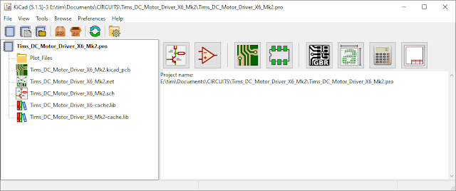
The first window that opens is the Project Manager.
On the right of the Manager are the buttons that will open the stand alone
Tools for creating your PCB. To the left is where you create and manage
all your files.
There are two ways to start a project. "Create New Project" and "Create New
Project From Template".
The "Create New Project From Template" is something to use one you have become
used to using KiCAD.
So for now, click "Create New Project" .
This opens the standard File Dialog.
Make sure that the Checkbox in the lower left of the Dialog Window is Checked.
This will create a folder with the name you have given your project and all
the files for your project will be created inside this folder.
Click save.
The Project Manager should now be populated with files like I have shown
above.
The next ting to do is Create/Edit our Schematic.
Click the "Schematic Layout Editor" icon in the right side of the
Project manager.
This opens the "Schematic Layout Editor"
This is where we place all the components and connect them to each other.
To place a component (symbol) in the editor, click the "Place
Symbol" icon on the right of the editor.
The "Choose Symbol" Window will open.
If this is the first time you have chosen a command that uses the database,
it may take a little time to open.
The first time you use a command that uses the database, it will load the
database into memory. Depending on how big you make the database, depends on
how long it takes to load.
The "Choose Symbol" Window is where you select the component you want to add
to the circuit.
You can type what you are looking for in the filter textbox.
Once you have found the symbol for the component you want to add to the
circuit, in the bottom right of the "Choose Symbol" Window you can also
chose the type of Footprint the component has.
Once you have selected the component you want, click OK and place it in the
circuit where you want.
Once you have placed all you components in the "Schematic Layout
Editor" you need to connect each of them to which ever component they
connect to.
To do this, use the "Place Wire" tool.
Now that the circuit is done, the next step is to position all the
components on a board which will become our PCB (Printed Circuit Board).
But before we can use the "PCB Layout Editor" we need to create a "Net List"
of all the components.
The "Net List" is similar to a bill of quantities but with extra information
like which component is connected to which.
To make sure that all components have been annotated with a unique
names/reference, the "Annotate Schematic symbols" tool can be used.
Clicking the "Annotate Schematic symbols" tool button brings up
a window where you can select options on how the schematic is Annotated.
Just click "Annotate" button, then the "Close" button.
With all the components annotated a Net List can be made.
This is just simply a matter of clicking the "Generate Netlist"
button.
An Options window will open first, click the "Generate Netlist" button.
A file dialog window will open to select a name for the Net List and where
to save it.
I just use the default it provides. Click the "Save" button.
The Options window will close automatically when the file is saved.
If the annotation of the schematic symbols had not been done, you would be
prompted to do so before creating the Net List.
Now that the Net List has been created, it's time to create the PCB.
Click the "PCB Layout Editor" icon in the right side of the Project manager.
This opens the "PCB Layout Editor"
As I have mentioned I am being very basic with the
instruction to using
KiCAD.
I will be mentioning the basics and what I think is an important part for
getting the board made by PCBWay.
When the "PCB Layout Editor" first opens, it will not be populated like
the image above, it will be empty.
The first thing to do it import all the components from the Net List.
Click the "Load Netlist" button at the top of the "PCB Layout Editor".
This will bring up the "Netlist" window.
The first time the "Netlist" window is opened, you will have to browse the
the netlist file.
Do this by clicking the folder icon in the top left corner. this will
bring up the standard file dialog window, chose the Netlist file created
earlier and click "open" button.
The "Netlist" window will load the Netlist file and list the changes that
will be applied.
Click the "Update PCB" button.
When you click the "Update PCB" button in the "Netlist" window, you will
find that all the components are attached to the mouse cursor.
Just place you mouse in a location on the page and click the left mouse
button.
Click a blank area of the page to deselect all the components.
You can now move and place each components on the page to where you want
them placed on the board.
To create a board, you use the "Edge.Cuts" layer, drawn with "Add Graphic
Lines" tool.
Select Edge.Cuts layer by using the dropdown list at the top of "PCB
Layout Editor" or by clicking the Edge.Cuts layer in the "Layers Manager"
on the right.
Use the "Add Graphic Lines" tool to draw the shape of you board.
The other "Add Graphic ...." tools can be used to draw more complex
shapes.
The "Add Graphic Circle" tool is used to insert holes.
The shape and size of the board is all done on the "Edge.Cuts" layer,
make sure there are no brakes in the drawing of the shapes.
Use the "Rout Tracks" to place the copper traces onto the board.
This can only be done on the Copper layers. F.Cu Layer is the Front
Copper Layer. B.Cu Layer is the Back Copper Layer. Select the
copper layer as you did for the Edge.Cuts.
You can add a Via using the "Add Vias" tool if you need to change
the side that the copper track runs.
After placing all your components and joining them all with copper
tracks you may want to write some text on the board.
You can do this using the "Add Text on Copper Layers or Graphic
Text"
This can be done on layers: F.Cu - Front Copper Layer. Text is written
with the copper on the board. B.Cu - Back Copper Layer. Text is written
with the copper on the board. F.SilkS - Front Silk Layer. Text is
written in ink over all coatings on the board. B.SilkS - Back Silk
Layer. Text is written in ink over all coatings on the board.
Remember when looking at text on the back of the board in the "PCB
Layout Editor", it will look mirrored (reversed), as the default view of
the board is viewed from the front.
One important thing to do when creating you board is to set the "Origin"
from which all dimensions and placement are made. Most manufacturers
preferer this to be set to the bottom left of your project.
To "Place the Auxiliary Axis Origin for some Plot File Formats and for
Drill and Place Files". Simply click this button and click where you
want it to be. Don't confuse it with the Add Layer Alignment Target.
Now that all is done, it's nice to have a look to see what it looks like.
In the top left of the "PCB Layout Editor" click on View, then choose "3D
Viewer"
This will open the "3D Viewer".
In the "3D Viewer" you can rotate zoom in/out and render the PCB.
The model used by the 3D viewer can also be ported to
FreeCad, to be
added to any 3D model you are making.
To get this made by
PCBWay, the next
step is to create some plot files they can use.
This is the easy part, it's just a matter of setting the right settings
and creating the files.
Click the "Plot (HPGL, PostScript, or GERBER format)" button in the top left
of the "PCB Layout Editor".
This will open the "Plot" window.
First thing is to create or set the output directory. Normally this is
called "Plot_Files".
Click the folder icon in the top right of the "Plot" window. This will open a
standard folder dialog window. Select/Create the folder to place the files in
and click "Select Folder".
In the top left you will see that the Plot Format is Gerber. This is the
type we want.
What you see above should be default. With one exception.
Also in general options you will see that "Use auxiliary axis as origin"
is checked. This is required.
Once you have all checked as shown above.
Click the "Plot" button. This will create the Gerber files for all the
layers we need.
Click the "Generate Drill Files" button. The "Generate Drill Files" window
will open.
The destination folder should be the same as set in the "Plot" dialog
window.
Make sure the selections are as above. Especially the "Drill Origin" is
set to Auxiliary Axis.
Click the "Generate Drill File" button. This will create the Drill File.
Close the "Generate Drill Files" window.
Close the "Plot" window.
In the Project Manager there is a button to open your project
folder, click it.
Open you plot folder.
Select all the files and create a ZIP File of them.
Name the ZIP File with the same name as your project. This is the file we
will use to order the BCB's from
PCBWay.
Time to place an order with
Go to there web site.
The top part of there home page should look like this:
As we are creating our PCB's from Gerber files.
We can go straight to the "PCB Instant Quote"
This will take us to this page.
It looks like a lot to fill in but the Gerber file we have created will do
most of the work for us. So the first thing to do is select this
option.
This alters the top of the page slightly.
We now have an option to upload Gerber Files.
Click the button to "+Add Gerber File"
This will open the standard File Dialog Window.
Brows to the ZIP File created in our project.
Select the file and open.
The top section of the page changes again.
It states if the upload of the Gerber files where a success.
It also shows you the front and back of your PCB.
In the top right of the form, you will see a link to a Gerber Viewer.
This will open in a new page and you will need to upload the ZIP File
again.
With the Gerber viewer you can check all the layers that make up
the PCB.
If you are assembling the SMD (Surface Mounted Devices) on your PCB your
self, then there is a tool you need.
You will find it very difficult to mount your components without it, I
cannot emphasise it enough.
Unless you have a laser cutter to make your own, then you need to purchase
an "SMD Stencil".
If all your components are TH (Through Hole) components, it's not
required.
I will be showing what a Stencil is used for later.
So if you look at the bottom of the form, you will see a checkbox
for an "SMD Stencil"
Check this box.
The bottom of the form will change to show details of what type of stencil
you want.
All that is left, is to create an account if you don't have one.
Select what postage you want.
And pay.
I had no issues using China Post.
Took a little time to arrive, no longer than buying items from eBay.
If you are signing up for the first time, you should also check if you
have received any discount vouchers for first time customer.
Received
Good Packing.
Vacuumed Sealed.
Top
Bottom
Darkness of solder tabs is due to bad lighting, the quality is
exhalent, just as I wanted.
Assembly
The first thing to do is fit the SMD's to the board.
SMD's are not soldered to a PCB in the normal way you solder TH (Through
Hole) components to a circuit board.
A soldering iron and a real of fluxed solder is not the best option.
You could try if you want, but there is an easier way.
Commercially SMD's are set in place using solder paste and placed in an
oven.
When the solder paste melts (at a lower temperature than normal solder)
the flux cleans the components, the solder pools and capillary action
happens which pulls the component into place and hold it there until the
solder cools and sets.
As I am just a hobbyist and this is my first time with SMD's on a
commercial board, I don't have PCB oven, so I will be using a heat gun,
not one of those for stripping paint, a small pen like tool. This is
what I have:
It's a butane torch that has several tip attachments. The tip fitted is
designed to just blow hot air.
There is some degree of adjustment, using this, it's best to have it at
low setting, the force of the the air blown out of the end is
proportional to the heat of the flame.
If it is set to high, the force of the air blown out of the end will
blow your components off the board.
It needs to be held at a distance where the force of the air is weak,
but it gives lots of heat over quit a large area around your components.
As I have mentioned, solder paste is used to attach the SMD's to the
board.
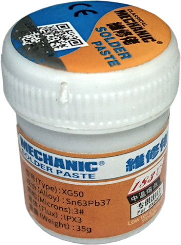
I just got a small 35g tub. The type I got has 183ºC on it so I guess
that's the melting temperature.
Type: XG50
Alloy: Sn63Pb37
Microns; 3#
Flux: IPX3
I think there is other stuff in it, to make it workable. The container
comes sealed when you get it.
I have noticed it tends to get a dry feel to it if left in the open air
for a time, so I would keep the lid on the container when not in use.
An SMD Stencil enables you to apply the right amount of Solder Paste to
you PCB.
You use it the same way
silk screen
process works.
I used a piece of clear plastic I am able to cut it with my 2W laser
when I make the surface dark using a White Board Marker.
White Board Markers have an ink that wipes away with a soft cloth or
tissue.
Once cut a jig needs to be made so that you can line up you PCB with the
Stencil.
Make sure the SMD-Stencil will not move position when placed over the PCB.
The tape holding the SMD-Stencil acts like a hinge.
As the components are very small.
I use an old pill tray to have all the components sorted.
I also printed a guide for placing the components.
Time to add the Solder Paste.
Spread the Solder Paste so that all the holes in the SMD-Stencil are
filled flush.
The area in the picture on the right is correct.
This gives the correct amount of Solder for each connection.
You can see this result more clearly when the SMD-Stencil is lifted.
Next step is to add the SMD's (Components)
I hold the PCB in a grip to hold the PCB level, also I want access later
to heat the underside.
Also being old my eyesight is not as good as it was so I use a magnifier
with light.
Once all the components are in place, heat the area around each
component with the hot air torch until the Solder Paste pools to a shiny
metallic bead.
When this happens the SMD should float slightly and align itself with the
pool of solder.
When this happens move to the next component.
Some times before you stat with the components it is best to heat the PCB
from underneath.
Making the PCB hot before heating the components, prevent to much heat
being applied to the component.
The last thing you want to do is melt the component.
Here is a video of how I solder the SMD's
After all SMD's are soldered to the PCB, next are the TH (Trough Hole)
components.
These are soldered in the normal way with a soldering iron and flux
solder.


 Click the "Schematic Layout Editor" icon in the right side of the
Project manager.
Click the "Schematic Layout Editor" icon in the right side of the
Project manager.


 Click the "PCB Layout Editor" icon in the right side of the Project manager.